
完全な内訳を受け取ります。 eCad ファイルで製品のフットプリントなどを確認してください。
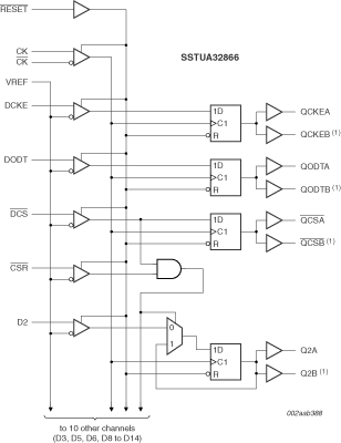
The SSTUA32866 is a 1.8 V configurable register specifically designed for use on DDR2 memory modules requiring a parity checking function. It is defined in accordance with the JEDEC standard for the SSTUA32866 registered buffer. The register is configurable (using configuration pins C0 and C1) to two topologies: 25-bit 1 : 1 or 14-bit 1 : 2, and in the latter configuration can be designated as Register A or Register B on the DIMM.
The SSTUA32866 accepts a parity bit from the memory controller on its parity bit (PAR_IN) input, compares it with the data received on the DIMM-independent D-inputs and indicates whether a parity error has occurred on its open-drain QERR pin (active LOW). The convention is even parity, that is, valid parity is defined as an even number of ones across the DIMM-independent data inputs combined with the parity input bit.
The SSTUA32866 is packaged in a 96-ball, 6 x 16 grid, 0.8 mm ball pitch LFBGA package (13.5 mm x 5.5 mm).
|
|
|
|
|
|
|
|---|---|---|---|---|---|
|
|
|
|
|
|
|
|
|
|
|
|
|
|
|
|
|
|
|
|
|
|
|
|
|
|
|
|
|
|
|
|
|
|
|
|
|
|
|
|
|
|
|
|
|
|
|
|
|
|
|
|
|
|
|
|
|
|
|
|
|
|
|
|
|
|
|
|
|
|
2 ドキュメント
コンパクトリスト
完全な内訳を受け取ります。 eCad ファイルで製品のフットプリントなどを確認してください。
There are no recently viewed products to display.
閲覧履歴を表示または編集する