セレクタ・ガイド (1)
-
Analog Automotive and Industrial Selector Guide[INDCONTANLPRDFL]
This part is not recommended for new designs. For new designs, we recommend UJA1169ATK.
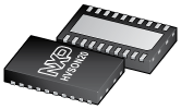
The UJA1169 is a mini high-speed CAN System Basis Chip (SBC) containing an ISO 11898-2:201x (upcoming merged ISO 11898-2/5/6) compliant HS-CAN transceiver and an integrated 5 V or 3.3 V 250 mA scalable supply (V1) for a microcontroller and/or other loads. It also features a watchdog and a Serial Peripheral Interface (SPI). The UJA1169 can be operated in very low-current Standby and Sleep modes with bus and local wake-up capability.
The UJA1169 comes in six variants. The UJA1169TK, UJA1169TK/F, UJA1169TK/X and UJA1169TK/X/F contain a 5 V regulator (V1). V1 is a 3.3 V regulator in the UJA1169TK/3 and the UJA1169TK/F/3.
The UJA1169TK, UJA1169TK/F, UJA1169TK/3 and UJA1169TK/F/3 variants feature a second on-board 5 V regulator (V2) that supplies the internal CAN transceiver and can also be used to supply additional on-board hardware.
The UJA1169TK/X and UJA1169TK/X/F are equipped with a 5 V supply (VEXT) for off-board components. VEXT is short-circuit proof to the battery, ground and negative voltages. The integrated CAN transceiver is supplied internally via V1, in parallel with the microcontroller.
The UJA1169xx/F variants support ISO 11898-6:2013 and ISO 11898-2:201x compliant CAN partial networking with a selective wake-up function incorporating CAN FD-passive.
CAN FD-passive is a feature that allows CAN FD bus traffic to be ignored in Sleep/Standby mode. CAN FD-passive partial networking is a good fit for networks that support both CAN FD and classic CAN communications. It allows normal CAN controllers that do not need to communicate CAN FD messages to remain in partial networking Sleep/Standby mode during CAN FD communication without generating bus errors.
The UJA1169 implements the standard CAN physical layer as defined in the current ISO11898 standard (-2:2003, -5:2007, -6:2013). Pending the release of the upcoming version of ISO11898-2:201x including CAN FD, additional timing parameters defining loop delay symmetry are included. This implementation enables reliable communication in the CAN FD fast phase at data rates up to 2 Mbit/s.
A dedicated LIMP output pin is provided to flag system failures.
A number of configuration settings are stored in non-volatile memory. This arrangement makes it possible to configure the power-on and limp-home behavior of the UJA1169 to meet the requirements of different applications.

| | | | | |
|---|---|---|---|---|---|
| | | | | |
| | | | | |
| | | | | |
| | | | | |
| | | | | |
| | | | | |
| | | | | |
| | | | | |
| | | | | |
| | | | | |
UJA1169TKクイック・リファレンス ドキュメンテーションの種類.
3 ドキュメント
コンパクトリスト
この選択アイテムには該当する結果がありません。
サインイン 許可されたセキュアファイルにアクセス。について詳しくはこちら セキュアなアクセス権.
セキュアファイルの読み込み中、しばらくお待ちください。
4 ドキュメント
コンパクトリスト